Cybot Processor 1 Board
 This
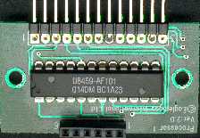
is the circuit diagram of the Processor 1 Board, it uses an Elan EM78P459
processor. Unfortunately, being a
mask programmed (or at least an OTP) micro-controller, it's difficult to really know how it
works, as it's entirely dependent on the internal programming. However, we
can make some reasonably educated guesses!. This
is the circuit diagram of the Processor 1 Board, it uses an Elan EM78P459
processor. Unfortunately, being a
mask programmed (or at least an OTP) micro-controller, it's difficult to really know how it
works, as it's entirely dependent on the internal programming. However, we
can make some reasonably educated guesses!.
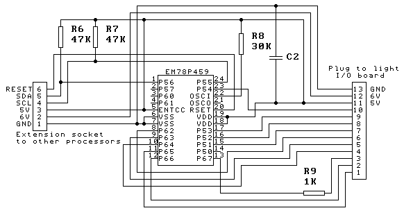
As
there's no external oscillator components (other than a 30K resistor to
the OSCI pin), this presumably means it's using it's internal oscillator
(unless there's a capacitor hidden away somewhere?). Checking with an
oscilloscope on pin 22 (OSCI) shows no oscillation, so that seems to
confirm it's using the internal RC oscillator.
The
outputs to the motor driver board are on pins 15, 16, 17, and 23, while
two of these are PWM enabled, they appear to be using software PWM.
Checking with the oscilloscope shows that Cybot is
running at half speed in light following mode (50% duty cycle on pins 15
and 17), presumably the PWM hardware isn't used as it wouldn't be possible
to provide speed control in both directions with the existing driver
hardware.
The
inputs from the LDR's are on pins 9 and 10, and although these pins are
capable of being used as A2D converters, they appear to be simply used as
digital inputs to time how long it takes to charge the two capacitors
(C10, C11 on the I/O board) through the LDR's, the associated discharge resistors
are R21, R22 also on the I/O board. Again, checking with the
oscilloscope shows a narrow ramp waveform on these pins, which gets wider
as you restrict light to the LDR's - more resistance, longer charging
time.
The
two resistors R6 and R7 look to be the pull-up resistors for an I2C type
bi-directional bus, presumably this will be used to communicate
between the various processors as Cybot develops?. The six pin connector
also carries the GND, 6V and 5V rails, plus the reset line for the
processor - this has caused problems on some boards, and it's been
suggested that plugging a 47K 1/8W resistor between pins 6 (Reset) and 3
(+5V) will help to make the board work - to date there's been no official
announcement, but my board seems much! happier with it fitted!. According to the
datasheet 47K is actually too high, they specify no greater than 40K, and
anything from 40K down to a shorting link should be fine. It's extremely
bad practice to leave the reset pin floating, and presumably there will be
a pull-up on one of the later boards - or perhaps a complete 'brown-out'
circuit.
Following
the release of the Processor 2 board, I've been doing some more tests on
the bus between the processors, pin 4 appears to be the clock, and pin 5
the data, and it's not a standard I2C interface, with I2C both lines are
normally high, and processors 'call' for attention by bringing them low -
this isn't done, the data line is normally high, but the clock line is
normally low. In 'line following' and 'light seek' modes you only get a
short burst of data, as the mode switch setting is fed back to the
Processor 1 board - however, in sonar modes there is a regular stream of
data, with sixteen positive clock pulses on pin 4, and the associated data
on pin 5. This data changes every few seconds, following a 'beep' from
Cybot, to one of two different values, but it's hard to know what's going
on without the rest of the sonar hardware due to arrive in issue 14.
This
leaves two other components, C2 - which is a power supply decoupling
capacitor, and R9, which is fed from pin 13, and along with pin 12 feeds
the BZ socket on the I/O board. Presumably BZ means 'buzzer', and is the
connection for Cybot's piezo loudspeaker? - the 1K resistor will limit the
current drawn by this device. Feeding the piezo speaker from 2 pins allows
it to be fed with double the voltage, by taking one pin low, and the other
high, then reversing them, it gives 10v p-p drive for the sounder, from a
5v supply - this is known as a 'bridged' configuration, and is commonly
used in car stereos to give 4 times the power available from a single
ended amplifier stage..
If
you want to investigate the circuit further, you can download the
processor datasheet from the manufacturers
website, or direct from mine.
In
Issue 23 Eaglemoss replaced the original Processor 1 board with a
new one, this one uses a 20 pin processor instead of the previous 24 pin
one, It's actually an SPMC02A from Sun Plus Technology Co. Ltd.
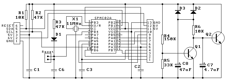
This
board is somewhat more complicated than the previous one, it includes an
external ceramic resonator for the clock oscillator, and has an external
reset network with a small socket for connection to a future board. It
also includes two small capacitors on the inputs from the LDR's,
presumably to reduce noise upsetting the readings. But the main change is
the circuit added to the right of the processor, incorporating Q1 and Q2,
I've no idea what it's supposed to do, I suspect it's a 'brown-out'
circuit, to help the processor reset more reliably on poor supplies - but
I don't see how C7 or C8 can receive any charging current, even when Q1
turns off as the supply drops away - I've checked the circuit repeatedly,
and as far as I can tell this is all there is!. I've even tried shorting
our R5, thus removing the drive to Q1, the collector of Q1 still stays at
zero volts though! (as I expected, with no visible charging path for C7).
I can only imagine there is a mistake on the board, or I'm missing
something!.
If
you want to investigate the circuit further, you can download the
processor datasheet from the
manufacturers
website.
|